
|
Contact Resistance Structures
The metal to semiconductor contacts for the ECE 444 mask set were intentionally made rather small so that the contact resistance can be easily measured.
In any structure or device, contact must be made to the device from the "outside world." Contact resistance exists between the test probe and the aluminum pad and between the aluminum pad and the silicon. We will ignore the contact resistance between the probe and pad, and concentrate on the resistance between the pad and the silicon. Contact resistance is determined by
- The size and shape of the contact,
- The distance between the edge of the contact window and the edge of the diffused region,
- The silicon type and doping concentration,
- Annealing
- The direction of current flow. (ref. 1)
To be able to predict the performance of devices and to design devices properly, it is necessary to determine the contact resistance. The mask set has been designed using a standard contact hole of 10 x 10 μm. Some contacts are larger, but they are only used for biasing, and will not affect device performance. In this unit you will measure the contact resistance using three methods and will explore smaller contacts of 5 and 2.5 μm square.
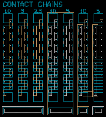
Contact Chains2
Theory
The first test structure is the contact chain (see Figure above). It is composed of
alternating diffused and aluminum regions. Since the resistance of the aluminum regions is very low,
it can be neglected. However, contact resistance and the resistance of the diffused regions
will be measured.
The contact chain is often used to test the integrity of contacts. A contact chain with
thousands of contacts will be fabricated and the integrity of all the contacts can be easily
tested with one measurement. If only one of the contacts is faulty, the structure will be an
open circuit. Contact chains are often included in test chips for yield analysis or reliability
studies3.
The structure can be split up into twelve blocks, each with one diffused region and two contacts.
The total resistance is the following:
Rtotal = 12 Rblock
The resistance of each block is determined by a geometry correction factor times the sheet
resistance plus the contact resistance:
Rblock = h Rs + 2 Rc
The diffused regions are 100 μm between contacts and 50 μm wide. Therefore, h is approximately
2 for this layout4.
Measurement
Fit a line to an I-V plot of each of the contact chains and record the resistance.
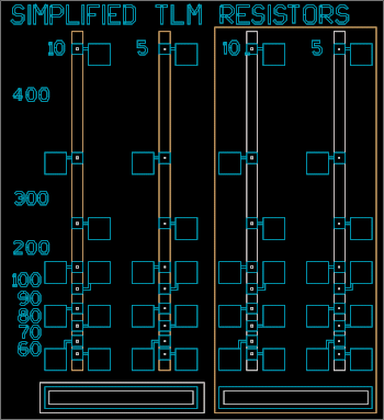
Transfer Length Method5
Theory
The second structure is a simplification of the Transfer Length Method (TLM) originally proposed by
Shockley (see Figure above). The structure allows you to measure various length resistors with
either 10 or 5 μm square contacts. The resistance values can be plotted against the resistor
length, and a line may be fit and extrapolated to a resistor of zero length. The result will be
twice the contact resistance (two contacts, one at each end).
Measurement
For each of the structures measure the resistance for each of the lengths: 400, 300, 200, 100, 90,
80, 70, and 60 μm. Later, you will fit a line through the points and extrapolate the line to a
resistor of zero length.
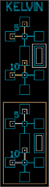
Kelvin Measurment Technique6
Theory
Finally, the Kelvin measurement technique may be used.
By forcing current between the pads b and d and measuring the voltage across pads a and c,
contact resistance can be determined. Since a relatively small current will flow between the
pads a and c, the voltage drop across the diffused region from pad a to the contact can be n
eglected. The contact resistance can be determined directly from:
Rc = (Va - Vc) / Ibd
Although this structure measures contact resistance the most directly, it is not perfect.
Results will be affected by effects from alignment and the enlarged diffused region around the
contact.
Measurement
Determine contact resistance for each of the four structures.
You may either select a specific current value and voltage, or fit a line.
Questions
The following questions pertain to only contact chains:
- Using the equations given in the theory section, determine the contact resistance
for each of the structures.
- Compare the 10 μm contact resistance in the diffusion one, diffusion two, and diffusion
one/two layers. Are they equivalent? Why or why not?
- Repeat question 2 for the 5 μm square contacts.
- The 5 μm square contacts are approximately one fourth of the area of the 10 μm square
contacts. You might reason that the contact resistance of the 5 μm square contacts
should be four times the contact resistance of the 10 μm contacts. Does your data
agree with this statement? Why or why not?
- There are several assumptions made when calculating contact resistance in this manner.
What are they? Do you feel that they are being satisfied?
- Large contact chains composed of thousands of contacts are often used to determine
the yield of the contacts in a commercial process. The 2.5 μm contacts are approaching
the limits of our process. Are all of your 2.5 μm contacts functional? It is possible
to process your wafer so 2.5 μm contacts are always functional. Why would this be
undesirable?
The following questions pertain to only the TLM structures.
- Plot resistance vs. length for each of the TLM structures. Determine contact resistance
which is one half of the y-intercept.
- Repeat question 2, 3, and 4 for the TLM structures.
The following question pertains to only the Kelvin measurement technique.
- Repeat question 7 for the Kelvin measurement structures.
The following questions pertain to all of the structures.
- Integrated circuits are getting smaller and smaller. Compare the advantages and
disadvantages of large and small contacts.
- Which of the structures do you think is the most reliable? Why?
- Does it appear that contact resistance is current dependent? If so, what do you
think is causing the current dependency?
References
- Badih El-Kareh and Richard J. Bombard, Introduction to VLSI Silicon Devices, (Kluwer
Academic Publishers, Hingham, Mass., 1986), pp. 38-40.
- Ping K. Ko, Robin R. Rudell, and Katalin Voros, "EECS 143 Processing and Design
of Integrated Circuits Laboratory Project," Memorandum No. UCB/ERL M88/50, Electronics
Research Laboratory, College of Engineering, University of California, Berkeley;
Berkeley, California, August 1988), Appendix V, pp 2-3.
- Simon S. Cohen and Gennady Sh. Gildenblat, VLSI Electronics Volume 13, Metal- Semiconductor
Contacts and Devices, Norman G. Einspruch, Editor, (Academic Press, Orlando, FL,
1986), p. 96.
- Simon S. Cohen and Gennady Sh. Gildenblat, Ibid.
- Dieter K. Schroder, Semiconductor Material and Device Characterization, (John Wiley
& Sons, Inc., New York, 1990), pp. 104-146.
- El-Kareh, et al., Ibid.
|
|
Devices
LASI was used for mask layout.
The mask set is currently under revision 1998: Dane Sievers, which is a minor redesign
of revision 1994: Ron Stack. All revisions are based on the work of revision 1991: Kevin Tsurutome.
Answers provided by this service may not be relevant to the materials presented in this website.
|