
|
Electrical Misalignment Structures
For most of the structures on the wafer to operate properly, the maximum misalignment
between any two layers must be less than 15 μm. For the small ring oscillator and
the CP FET to work, the maximum misalignment between any two layers must be less
than 7.5 μm. Rotational, or theta (θ), misalignment, will cause the x- and y-misalignments
to vary across the surface of the wafer. For example, one cell might be misaligned
by 4 μm, but on the other side of the wafer the misalignment might be 16 μm.
Theory
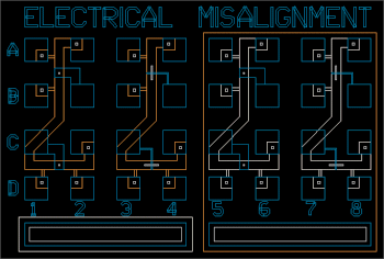
It is possible to electrically measure lithographic misalignment. The structure above
determines misalignment between layers in the x- and y- directions1. There are four
structures which measure misalignment between layers 1 and 4, 1 and 5,
2 and 4, and 2 and 5. The structure is basically a voltage divider. To determine
the misalignment between layers 1 and 4, current is forced through the ends, A2
and C2. Voltage is measured at each pad along the resistor: A1, B1,
B2, C1, D1,
and D2. The contact, B2, is designed to be exactly halfway between
A1 and B1. However,
misalignment will cause B2 to be off- center, and the measured voltage values can
be analyzed to determine the misalignment.
We can determine the amount of misalignment based on
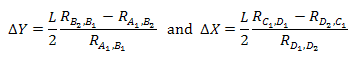
where L = 140 μm is the spacing betwen A1 and B1, and between D1 and D2.
Substituting V=IR
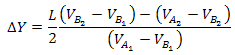
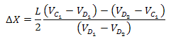
simplify
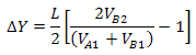
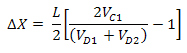
However, the diffused resistor must be operating linearly for these equations to
be valid.
Measurement
Force a current through the misalignment structures and measure the voltage at each
point.
Do this for each of the four structures.
References
1Badih El-Kareh and Richard J. Bombard, Introduction to VLSI Silicon Devices,
(Kluwer Academic Press, Hingham, Massachusetts, 1986), pp. 44-46.
Further Information
M. Feldman, "Alignment Techniques in Optical and X-Ray Lithography," VLSI Electronics:
Microstructure Science, Lithography for VLSI, Norman G. Einspruch and R. K. Watts,
Eds., (Academic Press, Orlando, FL, 1987), Vol. 16, Chap. 6, pp. 229-265.
|
|
Devices
LASI was used for mask layout.
The mask set is currently under revision 1998: Dane Sievers, which is a minor redesign
of revision 1994: Ron Stack. All revisions are based on the work of revision 1991: Kevin Tsurutome.
Answers provided by this service may not be relevant to the materials presented in this website.
|