
|
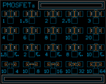
pMOSFETs
The pMOSFETs are tested in the lab using ICS, an automated testing program. For more information, see
Testing.
Theory
We can easily determine several characteristic parameters for the FETs, such as
gm (transconductance parameter), VT (threshold voltage), Leff
(effective length), (channel length modulation factor), and (body-bias coefficient).
There are three ways to determine threshold voltage.
- The first method utilizes a plot of transconductance, gm vs VG
for various VD. By extrapolating the curves when the device is in saturation
to the x-axis, we can determine the threshold voltage.
In saturation:
gm = Δ ID / Δ VG ~ (W / L) μ Ci (Vg-Vt)
gm = Δ ID / Δ VG ~ k (Vg - Vt),
where k is a constant including the channel length, L, width, W, capacitance per
unit area, Ci, and the average mobility, μ.
Therefore, (in saturation), at gm=0, Vg=Vt.
- Another method is to plot the square root of ID vs. Vg. By
extrapolating the saturated portion of the curves to the x-axis, we can determine
the threshold voltage.
In saturation:
ID = (1/2) k (Vg- Vt)2,
so sqrt(ID) = sqrt(k/2) (Vg-Vt), and at sqrt(ID)
= 0, Vg = Vt.
- The third method to determine threshold voltage is based on the transistor operating
in the linear region. By plotting ID vs. [Vg-VD/2], we can
read the threshold voltage off the x-intercept again.
ID = k [(Vg - Vt)VDS - (1/2) VDS2]
ID = k [(Vg-Vt)-VDS/2] VDS
= k [(Vg - VDS/2) - Vt] VDS
Then, when ID = 0, (Vg-VDS/2) = Vt
The body bias affects the threshold voltage, also. By determining the threshold
voltages for several body bias conditions, we can fit the Vt and VSB
into the following:
Vt = Vt0 + γ[(VSB + 2φF)1/2 - (2φF)1/2]
Vt ~ Vt0 + γ (VSB)1/2, when VSB
>> 2φF
From the traditional plot of ID vs. VD , we can determine
the channel length modulation factor.
ID ~ IDsat (1 + λ VDS)
where the x-intercept of the extrapolation of the I-V curves in saturation is the
reciprocal of the channel length modulation factor.
If two FETs are identical except for their channel lengths, then the effective channel
lengths can be obtained from measurements of Id vs. Vg in
saturation (|Vd| > |Vg - Vt|).
As in the first method above for determining Vt:
in saturation:
gm = d(Id )/ d(Vg) ~ (W / L) μ Ci (Vg-Vt),
with the channel length, L, width, W, capacitance per unit area, Ci,
and the average mobility, μ.
Then: gm' = d(gm) / d(Vg) ~ (W / L) μ Ci.
If the channel width, average mobility, and insulator capacitance per unit area
are the same for the two devices, then the ratios of the values of gm
' in saturation for the two devices is the ratio of the inverse of their channel
lengths:
gm1' / gm2' = Leff2 / Leff1
where the effective channel length Leff = Ldesign - ΔL.
If the causes of delta L are the same for both channel lengths (it is a reasonable
assumption that they would be for process related changes in the channel length),
then it is possible to find ΔL, since gm1', gm2', Ldesign1,
and Ldesign2 are known.
Further Information
- Schroder, Dieter K. Semiconductor Material and Device Characterization, New York:
John Wiley & Sons, 1990.
- Streetman, Ben G. Solid State Electronic Devices. Englewood Cliffs, NJ: Prentice-
Hall, Inc. 1980.
- Martin G. Buehler, VLSI Electronics Microstructure Science, Norman G. Einspruch
and Graydon B. Larrabee, Eds., (Academic Press, New York, 1983), Vol. 6, pp. 540-545.
|
|
Devices
LASI was used for mask layout.
The mask set is currently under revision 1998: Dane Sievers, which is a minor redesign
of revision 1994: Ron Stack. All revisions are based on the work of revision 1991: Kevin Tsurutome.
Answers provided by this service may not be relevant to the materials presented in this website.
|