
|
Process Control Structures
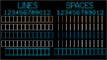
Lines and Spaces
Theory
The lines and spaces serve two purposes. During development, the lines and spaces indicate
the progress of development. As exposed photoresist develops, the lines tend to narrow and
disappear while the spaces tend to enlarge. The existence and size of the lines indicate the
quality of the photolithography.
The lines and spaces also monitor the etch process. All of our etches are isotropic;
therefore, for each micron etched in the vertical direction, one micron is etched in
the horizontal direction. The lines and spaces can be used to indicate the depth of
the etch and the quality of PR development.
For example, assume that the lines and spaces are accurately depicted by the photoresist
on the wafer. To completely etch a 1.5 μm thick oxide layer, we would expect to completely
etch away the three-micron line, but not the four-micron line assuming that any overdevelopment
was negligible. A gate designed to be 10 μm long will actually be different on your wafer due
to mask-making lithography (unlikely), mask duplication, PR development, oxide etching, and
lateral diffusion.
Measurement
After developing and etching each layer, note which lines and spaces are visible and intact on
your wafer using the PR microscope. Also note any anomalies, for example, "the three-micron
line is intact, but the four-micron line has a break in it."
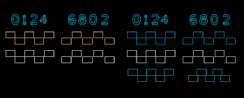
Etch Control Structures
Theory
The etch control structures are similar to the lines and spaces and can also be used to monitor
etches and PR development. The structures consist of adjacent boxes with spaces between the corners
of 0, 1, 2, 4, 6, 8, and 10 μm. The etch control structures can be used in the same way as the
lines to approximate the completeness of etch. If the corners of the boxes touch, then half of
the distance between the boxes the etch has been etched.
For example, if the fourth and fifth boxes are touching, than you have etched each box laterally
two microns. The fourth and fifth boxes are separated by 4 μm. Note which boxes are touching
after each etch.
The aluminum etch control structure is different. The aluminum boxes overlap by 0, 1, 2, 4, 6, 8,
and 10 μm since the boxes become smaller as the aluminum is etched.
Measurement
Note which boxes are touching for each level.
Surface Profilometer Structure

Theory
The surface profilometer structure is designed to be used with an stylus-type profilometer such
as the alpha step in the Microelectronics Laboratory. The structure allows you to measure the
oxide thickness and variations in the silicon surface. This structure will not be regularly
used by ece444 students, but may be used to diagnose problems.
Questions
- As mentioned in the notes, a 10 μm gate length designed on the mask will not result in a
10 μm gate length on your wafer. Assuming isotropic etching and the diffusion characteristics
learned in lecture, what gate length would you expect on your wafer from a 10 μm gate length
on the mask?
- Assuming that one micron line widths are the minimum feature size, what is the smallest
FET theoretically possible?
For additional information...
- Martin G. Buehler, "Semiconductor Measurement Technology: Microelectronic Test Pattern NBS-3 for Evaluating the Resistivity-Dopant Density Relationship of Silicon", NBS Special Publication 400-22. U.S. Department of Commerce, National Bureau of Standards, p. 33, (June 1976).
- L. B. Valdes, "Resistivity Measurements on Germanium for Transistors," Proc. IRE 42, 420-427 (1954).
|
|
Devices
LASI was used for mask layout.
The mask set is currently under revision 1998: Dane Sievers, which is a minor redesign
of revision 1994: Ron Stack. All revisions are based on the work of revision 1991: Kevin Tsurutome.
Answers provided by this service may not be relevant to the materials presented in this website.
|